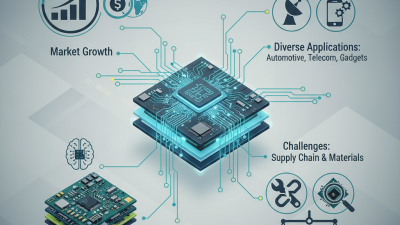
What is PCB Board Printing and How Does It Work?
PCB board printing is a critical aspect of electronics manufacturing. It involves creating printed circuit boards (PCBs) that serve as the backbone of electronic devices. Industry expert Dr. Emily Johnson once stated, "PCB board printing is where design meets functionality." This highlights the importance of precision in the production process.
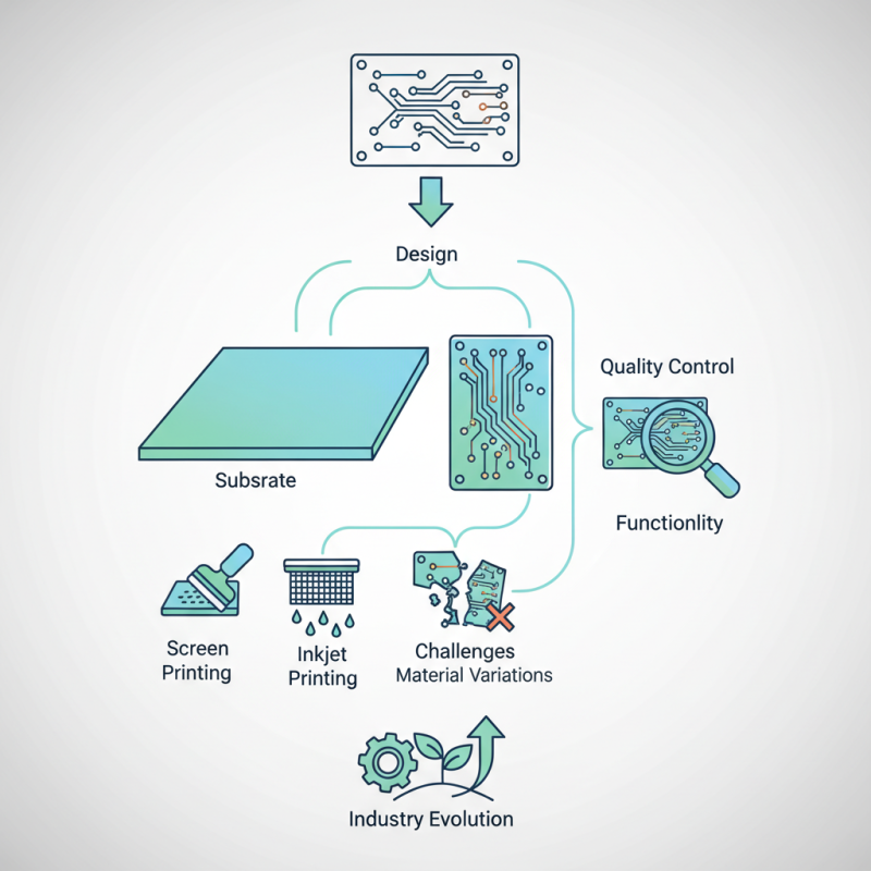
In PCB board printing, design elements are transferred onto a substrate. This includes intricate pathways and connecting points for electronic components. Different printing methods, such as screen printing and inkjet printing, can be used. Each method has its own benefits and challenges in terms of speed and accuracy.
While technology advances, there are still areas that require improvement. The process can be time-consuming, and quality control may not always be perfect. Variations in material quality can lead to defects. Despite these challenges, innovations in PCB board printing continue to evolve, driving the industry forward.
What is PCB Board Printing: Definition and Overview
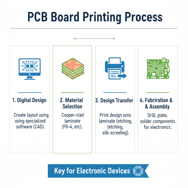
PCB board printing involves creating printed circuit boards (PCBs) that are essential in electronic devices. This process includes transferring designs onto a substrate using various techniques. It begins with a digital design, which can be created using specialized software. This design is later printed onto a copper-clad laminate.
The accuracy of the printing process is crucial. Any errors can lead to malfunctioning devices. Therefore, manufacturers often conduct tests to ensure high precision. They use methods like screen printing, inkjet printing, or even laser etching. Each technique has its pros and cons. For example, screen printing is suitable for larger production runs. However, it may struggle with intricate designs.
Despite advancements, challenges remain in PCB board printing. Material selection is vital. The wrong choice can cause issues like signal interference. Furthermore, environmental factors can affect the printing quality. Manufacturers must stay vigilant to maintain consistency. Awareness of these pitfalls leads to continuous improvement in this field.
The PCB Printing Process: Step-by-Step Explanation
The PCB printing process involves several critical steps. First, designing the layout is essential. Software tools help in crafting intricate circuits. These designs are often saved in formats like Gerber files, which serve as the blueprint for production. Importantly, industry reports indicate that well-executed designs reduce manufacturing costs by up to 30%.
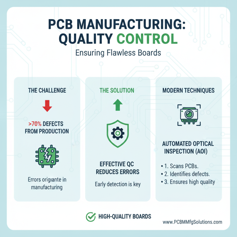
Next, the substrate material is prepared. Common materials include FR-4, which has excellent insulating properties. The printing begins with applying a layer of copper onto the substrate. High-precision machines etch the desired design onto this copper layer. This step is crucial; even minor errors can lead to failed circuits. In fact, analyses show that about 15% of PCBs fail during initial testing due to design flaws.
It’s essential to routinely check each step's output. Regular quality checks can save time and resources. Always ensure your designs are error-free before moving to production.
Tip: Use simulation software to visualize circuit performance early. This can highlight potential issues before physical production.
Tip: Keep your design files organized. Good file management reduces confusion and enhances collaboration.
Frequent reflection on production processes promotes continuous improvement, ultimately leading to superior PCB quality.
What is PCB Board Printing and How Does It Work?
| Step |
Description |
Tools/Materials |
| 1 |
Design the PCB layout using specialized software. |
PCB Design Software |
| 2 |
Print the design onto a film or stencil. |
Inkjet Printer, Film |
| 3 |
Apply the photo-sensitive coating to the copper board. |
Photoresist Coating |
| 4 |
Expose the PCB to UV light through the printed film. |
UV Light Source |
| 5 |
Develop the PCB to remove unexposed photoresist. |
Developer Solution |
| 6 |
Etch the copper to create the circuit pattern. |
Etching Solution (e.g., ferric chloride) |
| 7 |
Clean the PCB and remove the remaining photoresist. |
Cleaning Solution |
| 8 |
Test the finished PCB for functionality. |
Multimeter, Testing Equipment |
Key Materials Used in PCB Board Printing
Printed Circuit Boards (PCBs) are essential components in electronic devices. The process of PCB board printing involves several key materials. These materials play a crucial role in defining the performance and durability of the final product.
One primary material used in PCB printing is copper. Copper is often applied as a thin layer on the board. It serves as the electrical pathway, making connections between different components. Additionally, a substrate material, like fiberglass, provides structural support. This combination gives the PCB its rigidity and reliability.
Another important component is the solder mask. This is a protective layer that prevents short circuits and protects the copper traces. The ink used for solder masks comes in various colors, adding visual appeal as well. However, inconsistency in the thickness of the solder mask can lead to defects in production. Lastly, silkscreen ink is used for labeling. This ink can be prone to smudging if not applied correctly. Achieving the perfect balance with these materials can sometimes be challenging, requiring continuous adjustments in the printing process.
Future Trends and Innovations in PCB Board Printing Technology
The future of PCB board printing technology is vibrant and full of potential. Innovations in 3D printing methods are changing how we create circuit boards. These advancements allow for more intricate designs and faster production times. Additionally, materials used in PCB printing are evolving. Flexible circuits and biodegradable materials show promise for sustainable manufacturing.
Tips: Consider experimenting with new materials for unique design outcomes. The right materials can enhance performance and longevity.
Another trend is the integration of AI in the design process. AI helps optimize layouts and detect potential issues early. This reduces errors and saves time during production. However, as with any technology, reliance on AI raises concerns. Trusting algorithms too deeply can lead to oversight of important human factors.
Tips: Always review AI-generated designs critically. Ensure that human expertise is part of the process. This can prevent costly mistakes in production.