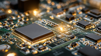
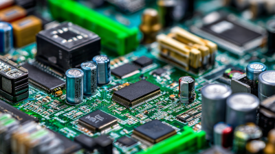
Common Issues Faced in High Density PCB Circuit Design
As the demand for more compact and efficient electronic devices continues to surge, the complexity of PCB circuit designs has also increased significantly. According to the IPC's "Design and Manufacturing Process Integrations" report, nearly 60% of engineers reported that high-density PCB circuit design poses significant challenges, particularly in managing heat dissipation and maintaining signal integrity. With advancements in technology such as 5G and IoT, the trend towards smaller and more integrated circuit boards is expected to be dominant in the future. However, these innovations come with their own set of challenges, including electromagnetic interference and routing difficulties, which can hinder performance if not properly addressed. This blog will explore the common issues faced in high-density PCB circuit design, providing insights into effective strategies and solutions to navigate this evolving landscape.
Common Design Pitfalls in High Density PCB Layouts
High-density PCB layouts present unique challenges that can significantly impact the performance and reliability of electronic devices. One common pitfall is the improper placement of components, which can lead to excessive electromagnetic interference (EMI). According to a report by IPC, up to 50% of PCB design failures can be attributed to poor component placement, making it crucial for designers to carefully consider the spatial arrangement of components to minimize noise and enhance signal integrity.
Another significant issue arises from inadequate routing strategies. High-density designs often lead to congested traces, increasing the risk of crosstalk and signal degradation. Data from the IEEE shows that improper routing can result in a 30% performance loss in high-speed circuits. Designers must prioritize the use of advanced routing techniques, such as controlled impedance and differential signaling, to maintain signal quality across densely packed traces. By addressing these pitfalls, PCB designers can optimize their layouts for both performance and manufacturability, ensuring their high-density PCBs meet stringent industrial standards.
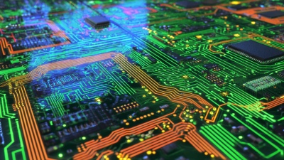
Strategies for Effective Signal Integrity in Complex Circuits
In high density PCB circuit design, ensuring effective signal integrity is crucial for the performance of complex circuits. According to a report by IPC, approximately 70% of PCB design failures are due to inadequate signal integrity management. This highlights the importance of employing advanced simulation tools and design techniques early in the design phase to predict and mitigate issues related to signal degradation, crosstalk, and electromagnetic interference (EMI). Designers should leverage time-domain reflectometry (TDR) and frequency-domain reflectometry (FDR) techniques to analyze and refine their layouts systematically.
One strategy for enhancing signal integrity is the implementation of stringent routing guidelines, including controlled impedance techniques. A study published in the IEEE Transactions on Components, Packaging, and Manufacturing Technology indicates that maintaining a consistent impedance is critical for high-speed signal transmission, leading to a 50% reduction in signal reflection in properly controlled environments. Additionally, utilizing differential pair routing can further minimize crosstalk and improve noise immunity, particularly in multilayer PCBs, which can have more complex interconnections. By adopting these strategies, designers can significantly enhance the reliability and performance of high-density PCB applications.

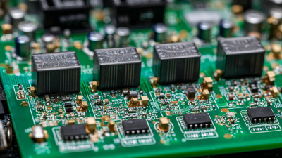
Thermal Management Challenges in High Density PCB Designs
In high density PCB designs, thermal management emerges as a critical concern that directly impacts performance and reliability. As components are packed closer together, the heat generated can lead to elevated temperatures, potentially causing failures or decreasing the lifespan of the circuit. Efficient thermal management strategies are essential to dissipate heat effectively and maintain optimal operating conditions. Techniques such as incorporating thermal vias, heat sinks, and strategically placing components can help to enhance heat dissipation.
Moreover, the choice of materials plays a significant role in thermal performance. Using substrates with better thermal conductivity can facilitate heat transfer away from hot spots. Designers must also consider airflow and thermal coupling between components; inadequate airflow can exacerbate heat buildup, leading to hotspots. Therefore, simulations and thermal analysis during the design phase are imperative to predict thermal behavior and identify possible issues before production. Engaging in proactive thermal management not only ensures functional integrity but also supports the overall longevity of high density PCBs.
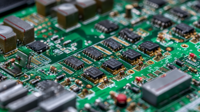
Best Practices for Component Placement in Compact Spaces
When designing high-density PCBs, component placement is at the forefront of challenges, especially given the constraints of compact spaces.
One of the best practices involves prioritizing the layout based on signal integrity.
For components that require frequent communication, such as microcontrollers or high-speed processors,
strategic positioning can reduce the length of critical traces, thereby minimizing interference.
It’s essential to create a layout that keeps sensitive components away from noisy elements like power regulators or motors.

Additionally, optimizing component orientation can significantly enhance thermal management and accessibility for testing and maintenance.
Implementing a staggered layout, where taller components are interspersed with shorter ones, allows for better air flow and heat dissipation.
Proper spacing, adhering to the recommended clearance, avoids overheating and ensures reliability in performance.
Furthermore, utilizing multi-layer designs can help in efficiently routing connections while maintaining a compact form, providing an effective solution to complex circuitry without compromising the overall design integrity.
Tools and Techniques for Efficient High Density PCB Testing
In the realm of high-density PCB circuit design, testing becomes a critical phase that ensures reliability and performance. With the intricate interconnections and compact layouts, traditional testing methods often fall short. This is where advanced tools and techniques come into play, transforming the complexity of high-density designs into manageable testing processes. Automated optical inspection (AOI) and X-ray inspection are vital methods that help detect hidden defects without physically accessing all components. These technologies offer a non-invasive approach to identify issues such as solder joint integrity and alignment errors.
Another important technique is the use of selective soldering and advanced rework tools, which are essential in maintaining performance quality in high-density boards. These tools not only enhance precision in soldering but also reduce the risk of damage to surrounding components. Additionally, employing simulation software before the physical testing phase can significantly streamline the design verification process, allowing engineers to preemptively identify potential failure points and mitigate risks before they materialize. As the demands for high-density PCBs continue to rise, investing in these cutting-edge tools and techniques becomes indispensable for ensuring optimal circuit functionality and longevity.
Common Issues Faced in High Density PCB Circuit Design
| Issue |
Description |
Tools |
Techniques |
| Signal Integrity |
Challenges with maintaining signal quality due to interference and crosstalk. |
SPICE simulators, Signal Integrity software |
Differential signaling, controlled impedance |
| Thermal Management |
Heat dissipation issues in densely packed circuits. |
Thermal analysis tools, Computational Fluid Dynamics (CFD) |
Heat sinks, thermal vias |
| Manufacturability |
Difficulty in producing high-density PCB designs with high yields. |
Design Rule Check (DRC) software |
DFM (Design for Manufacturability) practices |
| Testing Challenges |
Issues related to accessibility and testing points on dense boards. |
Automated test equipment (ATE), Boundary Scan testers |
Built-in self-test (BIST), fixtureless testing |
| Power Distribution |
Issues with providing sufficient power to densely packed components. |
Power Integrity analysis tools |
Decoupling capacitors, power plane design |